TL F 5977
CD4071BMCD4071BC
Quad
2-Input
OR
Buffered
B
Series
Gate
CD4081BMCD4081BC
Quad
2-Input
AND
Buffered
B
Series
Gate
February 1988
CD4071BM CD4071BC
Quad 2-Input OR Buffered B Series Gate
CD4081BM CD4081BC
Quad 2-Input AND Buffered B Series Gate
General Description
These quad gates are monolithic complementary MOS
(CMOS) integrated circuits constructed with N- and P-chan-
nel enhancement mode transistors They have equal source
and sink current capabilities and conform to standard B se-
ries output drive The devices also have buffered outputs
which improve transfer characteristics by providing very
high gain
All inputs protected against static discharge with diodes to
V
DD
and V
SS
Features
Y
Low power TTL
Fan out of 2 driving 74L
compatibility
or 1 driving 74LS
Y
5V � 10V � 15V parametric ratings
Y
Symmetrical output characteristics
Y
Maximum input leakage 1 mA at 15V over full tempera-
ture range
Connection Diagrams
CD4071B Dual-In-Line Package
TL F 5977 � 3
Top View
CD4081B Dual-In-Line Package
TL F 5977 � 6
Top View
Order Number CD4071B or CD4081B
C1995 National Semiconductor Corporation
RRD-B30M105 Printed in U S A
Absolute Maximum Ratings
(Notes 1
2)
If Military Aerospace specified devices are required
please contact the National Semiconductor Sales
Office Distributors for availability and specifications
Voltage at Any Pin
b
0 5V to V
DD
a
0 5V
Power Dissipation (P
D
)
Dual-In-Line
700 mW
Small Outline
500 mW
V
DD
Range
b
0 5 V
DC
to
a
18 V
DC
Storage Temperature (T
S
)
b
65 C to
a
150 C
Lead Temperature (T
L
)
(Soldering 10 seconds)
260 C
Operating Conditions
Operating Range (V
DD
)
3 V
DC
to 15 V
DC
Operating Temperature Range (T
A
)
CD4071BM CD4081BM
b
55 C to
a
125 C
CD4071BC CD4081BC
b
40 C to
a
85 C
DC Electrical Characteristics
CD4071BM CD4081BM (Note 2)
Symbol
Parameter
Conditions
b
55 C
a
25 C
a
125 C
Units
Min
Max
Min
Typ
Max
Min
Max
I
DD
Quiescent Device
V
DD
e
5V
0 25
0 004
0 25
7 5
m
A
Current
V
DD
e
10V
0 50
0 005
0 50
15
m
A
V
DD
e
15V
1 0
0 006
1 0
30
m
A
V
OL
Low Level
V
DD
e
5V
0 05
0
0 05
0 05
V
Output Voltage
V
DD
e
10V
l
I
O
l
k
1 mA
0 05
0
0 05
0 05
V
V
DD
e
15V
(
0 05
0
0 05
0 05
V
V
OH
High Level
V
DD
e
5V
4 95
4 95
5
4 95
V
Output Voltage
V
DD
e
10V
l
I
O
l
k
1 mA
9 95
9 95
10
9 95
V
V
DD
e
15V
(
14 95
14 95
15
14 95
V
V
IL
Low Level
V
DD
e
5V V
O
e
0 5V
1 5
2
1 5
1 5
V
Input Voltage
V
DD
e
10V V
O
e
1 0V
3 0
4
3 0
3 0
V
V
DD
e
15V V
O
e
1 5V
4 0
6
4 0
4 0
V
V
IH
High Level
V
DD
e
5V V
O
e
4 5V
3 5
3 5
3
3 5
V
Input Voltage
V
DD
e
10V V
O
e
9 0V
7 0
7 0
6
7 0
V
V
DD
e
15V V
O
e
13 5V
11 0
11 0
9
11 0
V
I
OL
Low Level Output
V
DD
e
5V V
O
e
0 4V
0 64
0 51
0 88
0 36
mA
Current
V
DD
e
10V V
O
e
0 5V
1 6
1 3
2 25
0 9
mA
(Note 3)
V
DD
e
15V V
O
e
1 5V
4 2
3 4
8 8
2 4
mA
I
OH
High Level Output
V
DD
e
5V V
O
e
4 6V
b
0 64
b
0 51
b
0 88
b
0 36
mA
Current
V
DD
e
10V V
O
e
9 5V
b
1 6
b
1 3
b
2 25
b
0 9
mA
(Note 3)
V
DD
e
15V V
O
e
13 5V
b
4 2
b
3 4
b
8 8
b
2 4
mA
I
IN
Input Current
V
DD
e
15V V
IN
e
0V
b
0 10
b
10
b
5
b
0 10
b
1 0
m
A
V
DD
e
15V V
IN
e
15V
0 10
10
b
5
0 10
1 0
m
A
Note 1
``Absolute Maximum Ratings'' are those values beyond which the safety of the device cannot be guaranteed Except for ``Operating Temperature Range''
they are not meant to imply that the devices should be operated at these limits The table of ``Electrical Characteristics'' provides conditions for actual device
operation
Note 2
All voltages measured with respect to V
SS
unless otherwise specified
Note 3
I
OH
and I
OL
are tested one output at a time
2
DC Electrical Characteristics
CD4071BC CD4081BC (Note 2)
Symbol
Parameter
Conditions
b
40 C
a
25 C
a
85 C
Units
Min
Max
Min
Typ
Max
Min
Max
I
DD
Quiescent Device
V
DD
e
5V
1
0 004
1
7 5
m
A
Current
V
DD
e
10V
2
0 005
2
15
m
A
V
DD
e
15V
4
0 006
4
30
m
A
V
OL
Low Level
V
DD
e
5V
0 05
0
0 05
0 05
V
Output Voltage
V
DD
e
10V
l
I
O
l
k
1 mA
0 05
0
0 05
0 05
V
V
DD
e
15V
(
0 05
0
0 05
0 05
V
V
OH
High Level
V
DD
e
5V
4 95
4 95
5
4 95
V
Output Voltage
V
DD
e
10V
l
I
O
l
k
1 mA
9 95
9 95
10
9 95
V
V
DD
e
15V
(
14 95
14 95
15
14 95
V
V
IL
Low Level
V
DD
e
5V V
O
e
0 5V
1 5
2
1 5
1 5
V
Input Voltage
V
DD
e
10V V
O
e
1 0V
3 0
4
3 0
3 0
V
V
DD
e
15V V
O
e
1 5V
4 0
6
4 0
4 0
V
V
IH
High Level
V
DD
e
5V V
O
e
4 5V
3 5
3 5
3
3 5
V
Input Voltage
V
DD
e
10V V
O
e
9 0V
7 0
7 0
6
7 0
V
V
DD
e
15V V
O
e
13 5V
11 0
11 0
9
11 0
V
I
OL
Low Level Output
V
DD
e
5V V
O
e
0 4V
0 52
0 44
0 88
0 36
mA
Current
V
DD
e
10V V
O
e
0 5V
1 3
1 1
2 25
0 9
mA
(Note 3)
V
DD
e
15V V
O
e
1 5V
3 6
3 0
8 8
2 4
mA
I
OH
High Level Output
V
DD
e
5V V
O
e
4 6V
b
0 52
b
0 44
b
0 88
b
0 36
mA
Current
V
DD
e
10V V
O
e
9 5V
b
1 3
b
1 1
b
2 25
b
0 9
mA
(Note 3)
V
DD
e
15V V
O
e
13 5V
b
3 6
b
3 0
b
8 8
b
2 4
mA
I
IN
Input Current
V
DD
e
15V V
IN
e
0V
b
0 30
b
10
b
5
b
0 30
b
1 0
m
A
V
DD
e
15V V
IN
e
15V
0 30
10
b
5
0 30
1 0
m
A
AC Electrical Characteristics
CD4071BC CD4071BM
T
A
e
25 C Input t
r
t
f
e
20 ns C
L
e
50 pF R
L
e
200 kX Typical temperature coefficient is 0 3% C
Symbol
Parameter
Conditions
Typ
Max
Units
t
PHL
Propagation Delay Time
V
DD
e
5V
100
250
ns
High-to-Low Level
V
DD
e
10V
40
100
ns
V
DD
e
15V
30
70
ns
t
PLH
Propagation Delay Time
V
DD
e
5V
90
250
ns
Low-to-High Level
V
DD
e
10V
40
100
ns
V
DD
e
15V
30
70
ns
t
THL
t
TLH
Transition Time
V
DD
e
5V
90
200
ns
V
DD
e
10V
50
100
ns
V
DD
e
15V
40
80
ns
C
IN
Average Input Capacitance
Any Input
5
7 5
pF
C
PD
Power Dissipation Capacity
Any Gate
18
pF
AC Parameters are guaranteed by DC correlated testing
Note 1
``Absolute Maximum Ratings'' are those values beyond which the safety of the device cannot be guaranteed Except for ``Operating Temperature Range''
they are not meant to imply that the devices should be operated at these limits The table of ``Electrical Characteristics'' provides conditions for actual device
operation
Note 2
All voltages measured with respect to V
SS
unless otherwise specified
Note 3
I
OH
and I
OL
are tested one output at a time
3
AC Electrical Characteristics
CD4081BC CD4081BM
T
A
e
25 C Input t
r
t
f
e
20 ns C
L
e
50 pF R
L
e
200 kX Typical temperature coefficient is 0 3% C
Symbol
Parameter
Conditions
Typ
Max
Units
t
PHL
Propagation Delay Time
V
DD
e
5V
100
250
ns
High-to-Low Level
V
DD
e
10V
40
100
ns
V
DD
e
15V
30
70
ns
t
PLH
Propagation Delay Time
V
DD
e
5V
120
250
ns
Low-to-High Level
V
DD
e
10V
50
100
ns
V
DD
e
15V
35
70
ns
t
THL
t
TLH
Transition Time
V
DD
e
5V
90
200
ns
V
DD
e
10V
50
100
ns
V
DD
e
15V
40
80
ns
C
IN
Average Input Capacitance
Any Input
5
7 5
pF
C
PD
Power Dissipation Capacity
Any Gate
18
pF
AC Parameters are guaranteed by DC correlated testing
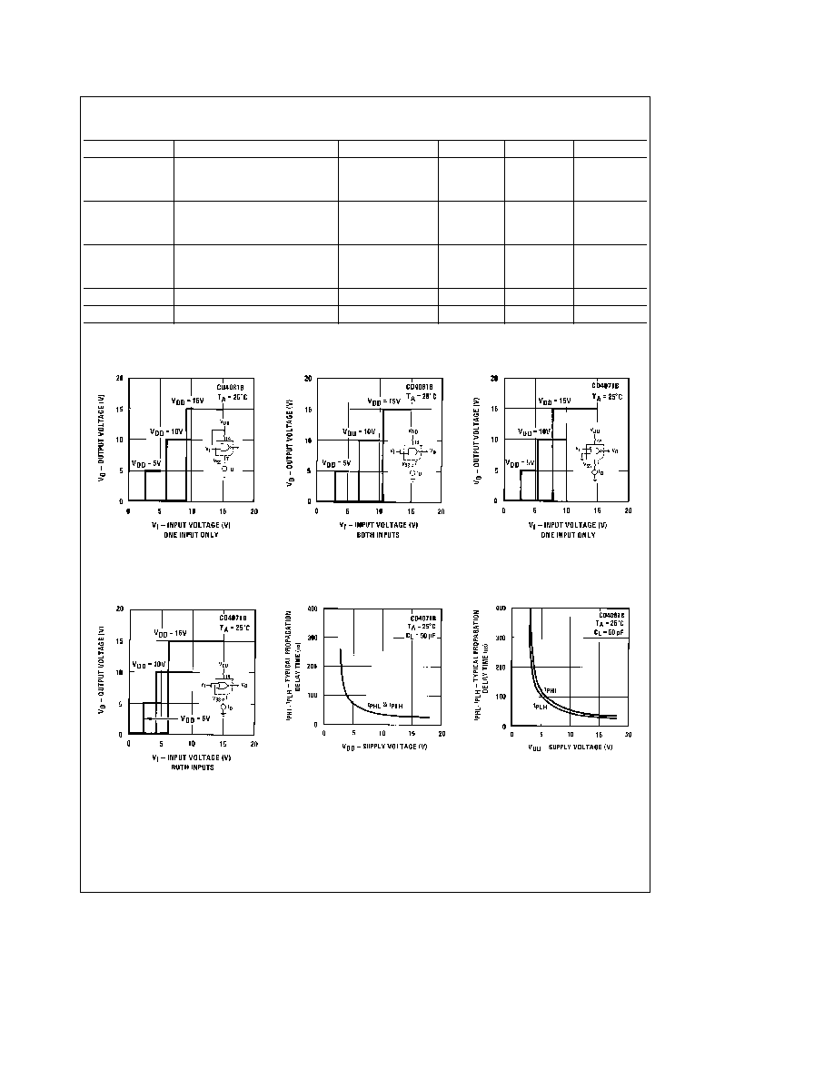
Typical Performance Characteristics
TL F 5977 � 7
FIGURE 1 Typical Transfer
Characteristics
TL F 5977 � 8
FIGURE 2 Typical Transfer
Characteristics
TL F 5977 � 9
FIGURE 3 Typical Transfer
Characteristics
TL F 5977 � 10
FIGURE 4 Typical Transfer
Characteristics
TL F 5977 � 11
FIGURE 5
TL F 5977 � 12
FIGURE 6
4
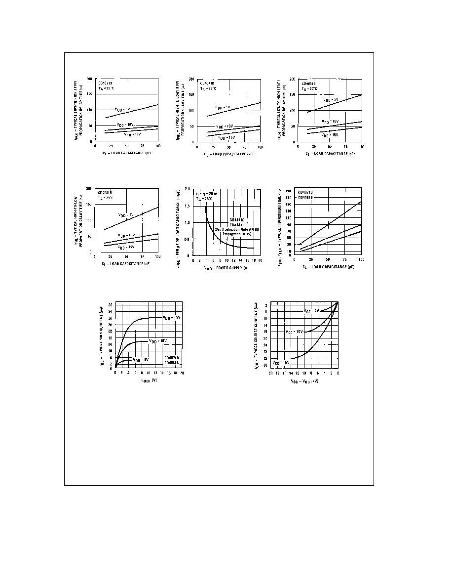
Typical Performance Characteristics
(Continued)
TL F 5977 � 13
FIGURE 7
TL F 5977 � 14
FIGURE 8
TL F 5977 � 15
FIGURE 9
TL F 5977 � 16
FIGURE 10
TL F 5977 � 17
FIGURE 11
TL F 5977 � 18
FIGURE 12
TL F 5977 � 19
FIGURE 13
TL F 5977 � 20
FIGURE 14
5
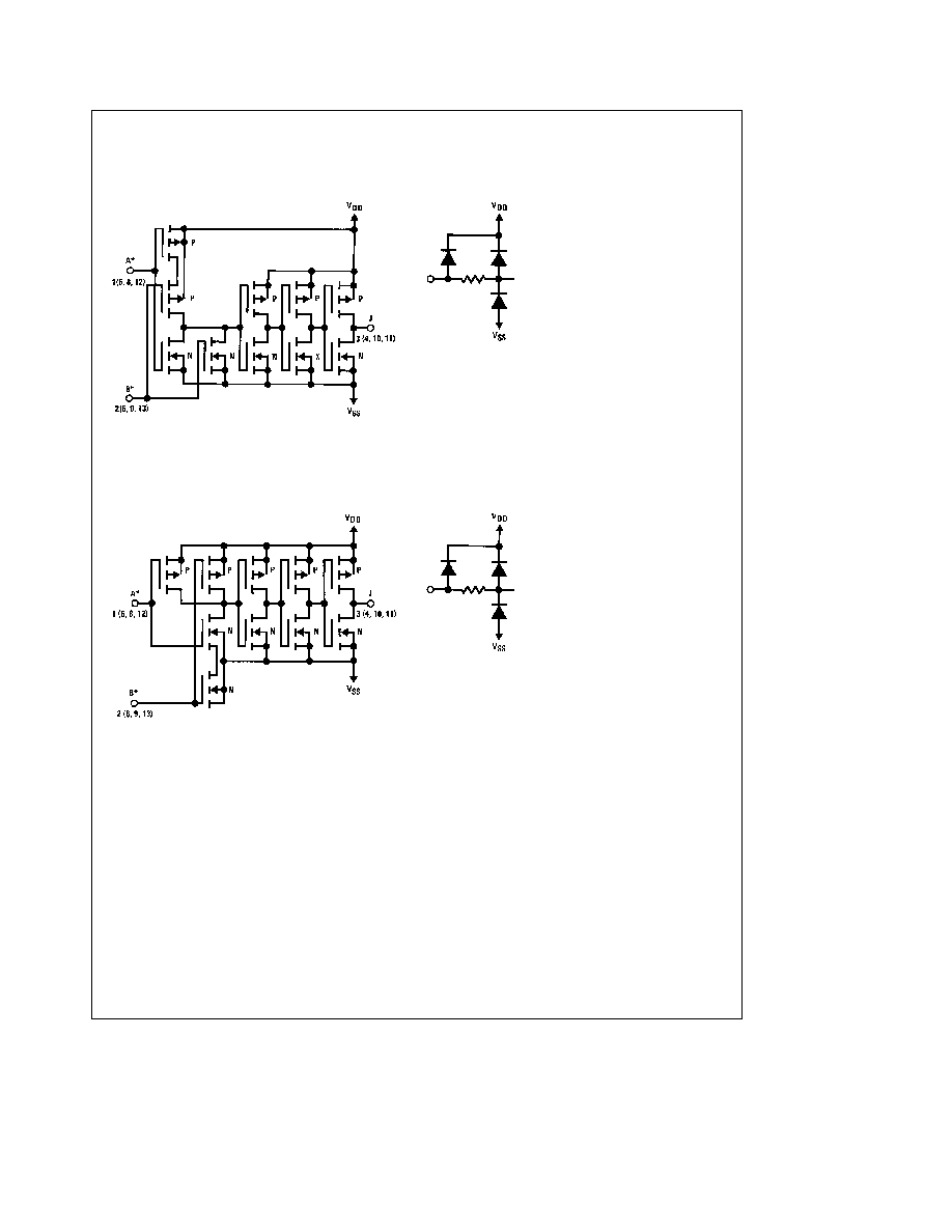
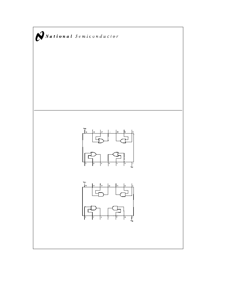
Schematic Diagrams
CD4071B
TL F 5977 � 1
TL F 5977 � 2
of device shown
J
e
A
a
B
Logical ``1''
e
High
Logical ``0''
e
Low
All inputs protected by standard
CMOS protection circuit
CD4081B
TL F 5977 � 4
TL F 5977 � 5
of device shown
J
e
A
B
Logical ``1''
e
High
Logical ``0''
e
Low
All inputs protected by standard
CMOS protection circuit
6
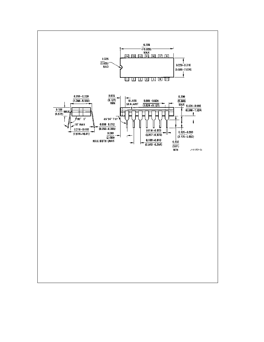
Physical Dimensions
inches (millimeters)
Ceramic Dual-In-Line Package (J)
Order Number CD4071BMJ CD4071BCJ
CD4081BMJ or CD4081BCJ
NS Package Number J14A
7
CD4071BMCD4071BC
Quad
2-Input
OR
Buffered
B
Series
Gate
CD4081BMCD4081BC
Quad
2-Input
AND
Buffered
B
Series
Gate
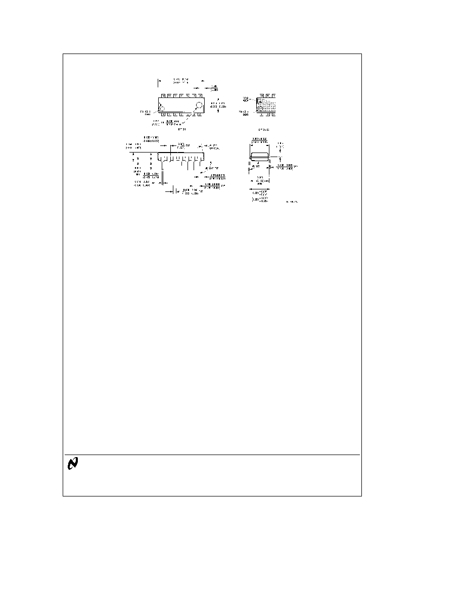
Physical Dimensions
inches (millimeters) (Continued)
Molded Dual-In-Line Package (N)
Order Number CD4071BMN CD4071BCN
CD4081BMN or CD4081BCN
NS Package Number N14A
LIFE SUPPORT POLICY
NATIONAL'S PRODUCTS ARE NOT AUTHORIZED FOR USE AS CRITICAL COMPONENTS IN LIFE SUPPORT
DEVICES OR SYSTEMS WITHOUT THE EXPRESS WRITTEN APPROVAL OF THE PRESIDENT OF NATIONAL
SEMICONDUCTOR CORPORATION As used herein
1 Life support devices or systems are devices or
2 A critical component is any component of a life
systems which (a) are intended for surgical implant
support device or system whose failure to perform can
into the body or (b) support or sustain life and whose
be reasonably expected to cause the failure of the life
failure to perform when properly used in accordance
support device or system or to affect its safety or
with instructions for use provided in the labeling can
effectiveness
be reasonably expected to result in a significant injury
to the user
National Semiconductor
National Semiconductor
National Semiconductor
National Semiconductor
Corporation
Europe
Hong Kong Ltd
Japan Ltd
1111 West Bardin Road
Fax (a49) 0-180-530 85 86
13th Floor Straight Block
Tel 81-043-299-2309
Arlington TX 76017
Email cnjwge tevm2 nsc com
Ocean Centre 5 Canton Rd
Fax 81-043-299-2408
Tel 1(800) 272-9959
Deutsch Tel (a49) 0-180-530 85 85
Tsimshatsui Kowloon
Fax 1(800) 737-7018
English
Tel (a49) 0-180-532 78 32
Hong Kong
Fran ais Tel (a49) 0-180-532 93 58
Tel (852) 2737-1600
Italiano
Tel (a49) 0-180-534 16 80
Fax (852) 2736-9960
National does not assume any responsibility for use of any circuitry described no circuit patent licenses are implied and National reserves the right at any time without notice to change said circuitry and specifications